prof.dr. L.K. Nanver
Electronic Components, Technology and Materials (ECTM), Department of Microelectronics
Biography
Lis K. Nanver has a masters degree from the University of Aarhus, Denmark, and PhD degrees from the Ecole Nationale Sup�rieure des T�l�communications (ENST), Paris, France, and Delft University of Technology, The Netherlands. She has since 1975 been involved in different aspects of research on silicon device integration and now heads a group on this subject at TU Delft, where she is a professor.
Her main research interests are new devices and integration processes, mainly for RF, microwave, or smart sensor applications. She has pioneered several new ultrashallow diode technologies using techniques such as epitaxy by chemical-vapor or metal-induced solid-phase deposition, excimer laser processing and substrate transfer. In the last few years the research on new pure-dopant CVD processes for creating extremely shallow diodes (PureB for Si and PureGaB for Ge devices) has resulted in several leading-edge applications such as high-linearity silicon-on-glass varactor diodes, Si photodiode detectors for low penetration-depth beams and low-leakage Ge-on-Si photodiodes. For this work her group has received several prizes including the 2010 IEDM Roger Haken Award.
Publications
- Amorphous silicon carbide nitride layer as an alternative to a disordered silicon surface to suppress RF/microwave losses
Evseev, S; Nanver, LK; Rejaei Salmassi, B; Milosavljevic, S;
Microelectronic Engineering,
Volume 125, pp. 2-7, 2014. - Robust UV/VUV/EUV PureB Photodiode Detector Technology with High CMOS Compatibility
L.K. Nanver; L. Qi; V. Mohammadi; K.R.M. Mok; W.B. de Boer; N. Golshani; A. Sammak; T.L.M. Scholtes; A. Gottwald; U. Kroth; F. Scholze;
Journal of Selected Topics in Quantum Electronics,
Volume 20, Issue 6, pp. pp.1-11, 2014. - Temperature Dependency of the Kinetics of PureB CVD Deposition over Patterned Si/SiO2 Surfaces
V. Mohammadi; N. Golshani; K.R.C. Mok; W.B. de Boer; J. Derakhshandeh; L.K. Nanver;
Microelectronic Engineering,
Volume 125, pp. 45-50, 2014. - A 270�1 Ge-on-Si photodetector array for sensitive infrared imaging
Sammak, A; Aminian, M; Lin Qi; Charbon, E; Nanver, LK;
In Optical Sensing and Detection III Vol. 9141. Proceedings of SPIE- International Society for Optical Engineering,
pp. 1-7, 2014. - Thickness evaluation of deposited pureb layers in micro-/millimeter-sized windows to Si
Mohammadi, V; Ramesh, S; Nanver, LK;
In Proceedings - 2014 IEEE International Conference on Microelectronic Test Structures,
pp. 194-199, 2014. - Local Loading Effect of The Pure-Boron-Layer Chemical-Vapor Depositions
V. Mohammadi; W.B. de Boer; T.L.M. Scholtes; L.K. Nanver;
ECS Transactions,
Volume 50, Issue 4, pp. 333-341, 2013. DOI 10.1149/05004.0333ecst. - VUV/Low-Energy-Electron Si Photodiodes with Post-Metal 400�C PureB Deposition
V. Mohammadi; L. Qi; N. Golshani; K. R. C. Mok; W. B. de Boer; A. Sammak; J. J. Derakhshandeh. van der Cingel; L. K. Nanver;
IEEE Electron Device Letters,
Volume 34, Issue 12, 2013. DOI 10.1109/LED.2013.2287221. - Effects of Annealing on Chemical-Vapor Deposited PureB Layers
K. R. C. Mok; A. H. G. Vlooswijk; V. Mohammadi; L. K. Nanver;
ECS Journal of Solid State Science and Technology,
Volume 2, Issue 9, pp. 413-417, 2013. DOI 10.1149/2.044309jss. - A novel silicon interposer for measuring devices requiring complex two-sided contacting
J. Derakhshandeh; N. Golshani; L.A. Steenweg; W. van der Vlist; L.K. Nanver;
In IEEE International Conference on Microelectronic Test Structures,
Osaka, Japan, pp. 43-46, 2013. - Silicon Drift Detectors for the detection of x-rays down to energies as low as 100 eV
Negin Golshani; Jaber Derakhshandeh; Agata Sakic; Lis Nanver;
In Micronano conference,
Ede, The Netherlands, 2013. - Electrical and optical performance investigation of Si-based ultrashallow-junction VUV/EUV photodiodes
S. Lei; S. Nihtianov; X. Sha; L.K. Nanver; A. Gottwald; F. Scholze;
IEEE Transactions on Instrumentation and Measurement,
Volume 61, Issue 5, pp. 1268-1277, 2012. DOI 10.1109/TIM.2012.2187029.
document - PureGaB p+n Ge diodes grown in large windows to Si with a sub-300 nm transition region
A. Sammak; W.B. de Boer; L. L. Qi K. Nanver;
Journal of Solid-State Electronics,
Volume 74, Issue 1, pp. 126-133, Aug. 2012. DOI 10.1016/j.sse.2012.04.023. - Lateral-transistor test structures for evaluating the effectiveness of surface doping techniques
L. Qi; G. Lorito; L.K. Nanver;
IEEE Transactions on Semiconductor Manufacturing,
Volume 25, Issue 4, pp. 581-588, 2012. DOI 10.1109/TSM.2012.2206834. - Surface-charge-layer sheet-resistance measurements for evaluating interface RF losses on high-resistivity-silicon substrates
S.B. Evseev; L.K. Nanver; S. Milosaviljevi_;
IEEE Transactions on Microwave Theory and Techniques,
Volume 60, Issue 11, pp. 3542-3550, Nov. 2012. DOI 10.1109/TMTT.2012.2215050. - High-efficiency silicon photodiode detector for sub-keV electron microscopy
A. Sakic; G. van Veen; K. Kooijman; P. Vogelsang; T.L.M. Scholtes; W.B. de Boer; J. Derakhshandeh; W.H.A. Wien; S. Milosavljevic; L.K. Nanver;
IEEE Transactions on Electron Devices,
Volume 59, Issue 10, pp. 2707-2714, Oct. 2012. DOI 10.1109/TED.2012.2207960. - Pattern dependency and loading effect of pure-boron-layer chemical-vapor deposition
V. Mohammadi; W.B. de Boer; T.L.M. Scholtes; L.K. Nanver;
ECS Journal of Solid State Science and Technology,
Volume 1, Issue 1, pp. Q16-Q20, 2012. DOI 10.1149/2.024201jss. - Temperature dependence of chemical-vapor deposition of pure boron layers from diborane
V. Mohammadi; W.B. de Boer; T.L.M. Scholtes; L.K. Nanver;
Applied Physics Letters,
Volume 101, Issue 11, pp. 1-4, 2012. DOI 10.1063/1.4752109. - A Ge-on-Si single-photon avalanche diode operating in Geiger mode at infrared wavelengths
M. Aminian; A. Sammak; L. L. Qi K. Nanver; E. Charbon;
In Proc. SPIE: Advanced Photon Counting Techniques VI,
Baltimore, Maryland, Apr 2012. DOI 10.1117/12.920561. - Epitaxial growth of large-area p+n diodes at 400 �C by aluminum-induced crystallization
A. Sakic; L. Qi; T.L.M. Scholtes; J. van der Cingel; L.K. Nanver;
In Proc. of the 42th European Solid-State Device Research Conference (ESSDERC 2012),
Bordeaux, France, pp. 145-148, Sept. 2012. ISBN 978-1-4673-1707-8; DOI 10.1109/ESSDERC.2012.6343354. - Modelling of electrical characteristics of ultrashallow pure amorphous boron p+n junctions
T. Knezevic; T. Suligoj; A. Sakic; L.K. Nanver;
In Proc. of the 35th International Convention MIPRO 2012,
Opatija, Croatia, pp. 36-41, May 2012. ISBN 978-1-4673-2577-6. - Electrical performance stability characterization of high-sensitivity Si-based EUV photodiodes in a harsh industrial application
L. Shi; S.N. Nihtianov; F. Scholze; L.K. Nanver;
In Proc. 38th Annual Conference on IEEE Industrial Electronics Society (IEEE IECON12),
Montreal, Canada, pp. 3952-3957, Oct 2012. ISBN 978-1-4673-2419-9; DOI 10.1109/IECON.2012.6389260. - Ge-on-Si: Single-crystal selective epitaxial growth in a CVD reactor
A. Sammak; W.B. de Boer; L.K. Nanver;
In Electro-Chemical Society (ECS) Meeting Abstracts,
Honolulu, Hawaii, Oct. 2012. - Impact of the Process and Chamber Parameters on CVD Deposition of PureB layer
V. Mohammadi; W.B. de Boer; T.L.M. Scholtes; L.K. Nanver;
In ICT.OPEN: Micro technology and micro devices (SAFE 2012),
Rotterdam, The Netherlands, Oct. 2012. - Pattern dependency of pure-boron-layer chemical-vapor depositions
V. Mohammadi; W.B. de Boer; T.L.M. Scholtes; L.K. Nanver;
In 221st ECS Meeting: ECS Transactions,
Seattle, Washington, pp. 39-48, May 2012. DOI 10.1149/1.3700937. - Insights to emitter saturation current densities of boron implanted samples based on defects simulations
K.R.C. Mok; R.C.G. Naber; L.K. Nanver;
In AIP Conf. Proc,
Valladolid, Spain, pp. 245-248, Jun. 2012. ISBN 978-0-7354-1108-1; DOI 10.1063/1.4766534. - Pure dopant deposition of B and Ga for ultrashallow junctions in Si-based devices
L.K. Nanver; A. Sammak; V. Mohammadi; K.R.C. Mok; L. Qi; A. Sakic; N. Golshani; J. Derakhshandeh; T.M.L. Scholtes; W.D. de Boer;
In ECS Trans. 2012: 27th Symposium on Microelectronics Technology and Devices (SBMicro2012),
Brazil, Brasilia, pp. 25-33, Aug. 2012. DOI 10.1149/04901.0025ecst. - Applications of PureB and PureGaB ultrashallow junction technologies
L.K. Nanver; A. _akic; V. Mohammadi; J. Derakhshandeh; K.R.C. Mok; L. Qi; N. Golshani; T.M.L. Scholtes; W.B. de Boer;
In 2012 IEEE 11th International Conference on Solid-State and Integrated Circuit Technology (ICSCT 2012),
Xi'an, pp. 303-306., Oct. 2012.
document - Low-pressure chemical vapor deposition of pureB layers on silicon for p+n junction formation
K.R.C. Mok; V. Mohammadi; L.K. Nanver; W.D. de Boer; A.H.G. Vlooswijk;
In 12th International Workshop on Junction Technology (IWJT 2012),
Shanghai, China, pp. 113-116, May 2012. DOI 10.1109/IWJT.2012.6212822. - Boron-layer silicon photodiodes for high-efficiency low-energy electron detection
A. _akic; L.K. Nanver; T.L.M. Scholtes; C.Th.H. Heerkens; T. Kne_evic; G. van Veen; K. Kooijman; P. Vogelsang;
Solid-State Electronics,
Volume 65-66, pp. 38-34, Dec. 2011. DOI 10.1016/j.sse.2011.06.042. - Integration of MOSFETs with SiGe dots as stressor material
L.K. Nanver; V. Jovanovic; C. Biasotto; J. Moers; D. Gruetzmacher; J.J. Zhang; N. Hrauda; M. Stoffel; F. Pezzoli; O.G. Schmidt; L. Miglio; H. Kosina; A. Marzegalli; G. G. Vastola. Mussler; J. Stangl; G. Bauer a;
Solid-State Electronics,
Volume 60, Issue 1, pp. 75-83., 2011. DOI 10.1016/j.sse.2011.01.038. - X-ray Nanodiffraction on a Single SiGe Quantum Dot inside a Functioning Field-Effect Transistor
N. Hrauda; J. Zhang; E. Wintersberger; T. Etzelstorfer; B. Mandl; J. Stangl; D. Carbone; V. Holy; V. Jovanovic; C. Biasotto; L.K. Nanver; J. Moers; D. Grutzmacher; G. Bauer;
Nano Letters,
Volume 11, Issue 7, pp. 2875-2880, 2011. DOI 10.1021/nl2013289. - Arsenic-doped high-resistivity-silicon epitaxial layers for integrating low-capacitance diodes
A. Sakic; T.L.M. Scholtes; W. de Boer; N. Golshani; J. Derakhshandeh; L.K. Nanver;
Materials,
Volume 4, Issue 12, pp. 2092-2107, Dec. 2011. DOI 10.3390/ma4122092. - Low-complexity full-melt laser-anneal process for fabrication of low-leakage implanted ultrashallow junctions
C. Biasotto; V. Gonda; L.K. Nanver; T.L.M. Scholtes; J. van der Cingel; D. Vidal; V. Jovanovi_;
Journal of Electronic Materials,
Volume 40, Issue 11, pp. 2187-2196, 2011. DOI 10.1007/s11664-011-1734-6. - Analysis of electrothermal effects in bipolar differential pairs
V. d'Alessandro; L. La Spina; L.K. Nanver; N. Rinaldi;
IEEE Transactions on Electron Devices,
Volume 58, Issue 4, pp. 966-978, Apr. 2011. DOI 10.1109/TED.2011.2106132. - Silicon Photodiodes for Low Penetration Depth Beams such as DUV/VUV/EUV Light and Low-Energy Electrons
L.K. Nanver;
In Advances Photodiodes,
InTech, Publishing, 2011. ISBN: 978-953-307-163-3. - PureB silicon photodiode detectors for DUV/VUV/EUV light and low-energy electrons
L.K. Nanver;
In Workshop on Next Generation UV Instrument Technologies Enabling Missions Astrophysics, Cosmology and Planetary Sciences,
Keck Institute for Space Studies, Jet Propulsion Laboratory, Caltech, Pasadena, CA, USA-oral presentation, Aug. 2011. - Electrical performance optimization of a silicon-based EUV photodiode with near-theoretical quantum efficiency
L. L. ShiK. Nanver; S. Nihtianov;
In 16th International Solid-State Sensors, Actuators and Microsystems Conference (TRANSDUCERS 2011),
Beijing, China, pp. 48-51, Jun. 2011. ISBN 978-1-4577-0157-3; DOI 10.1109/TRANSDUCERS.2011.5969130. - Lateral bipolar structures for evaluating the effectiveness of surface doping techniques
G. Lorito; L. L. Qi K. Nanver;
In Proc. of IEEE International Conference on Microelectronic Test Structures (ICMTS 2011),
Amsterdam, pp. 108-113, Apr. 2011. DOI 10.1109/ICMTS.2011.5976870. - Optimization of the perimeter doping of ultrashallow p+-n--n+ photodiodes
T. Kne_evi_; T. Suligoj; A. _aki_; L.K. Nanver;
In Proc. International Conventions MIPRO 2011,
Opatija, Croatia, pp. 44-48, May 2011. ISBN 978-1-4577-0996-8.
document - High-sensitivity high-stability silicon photodiodes for DUV, VUV and EUV spectral ranges
L. Shi; S. Nihtianov; L.K. Nanver; F. Scholze; A. Gottwald;
In O.H. Siegmund (Ed.), Proc. SPIE,
San Diego, CA, USA, pp. 1-9, Aug. 2011. DOI 10.1117/12.891865. - Solid-state backscattered-electron detector for sub-keV imaging in scanning electron microscopy
A. _aki_; L.K. Nanver; G. van Veen; K. Kooijman; P. Vogelsang; T.L.M. Scholtes; W. de Boer; W. Wien; S. Milosavljevi_; C.Th.H. Heerkens; T. Kne_evi_; I. Spee;
In Proc. ICT.OPEN: Micro technology and micro devices (SAFE 2011),
Veldhoven, The Netherlands, pp. 92-95, Nov. 2011. - Large-area selective CVD epitaxial growth of Ge on Si substrates
A. Sammak; W.B. de Boer; L. L. Qi K. Nanver;
In Proc. ICT.OPEN: Micro technology and micro devices (SAFE 2011),
Veldhoven, The Netherlands, pp. 96-99, Nov. 2011.
document - with transferring PureB CVD from an epitaxial reactor to a furnace system
K.R.C. Mok; L.K. Nanver; W.D. de Boer; A.H.G. Vlooswijk;
In Proc. ICT.OPEN: Micro technology and micro devices (SAFE 2011),
Veldhoven, The Netherlands, pp. 76-78, Nov. 2011. - On the uniformity of pure-boron-layer depositions
V. Mohammadi; W.D. de Boer; T.L.M. Scholtes; A. Sakic; C. Heerkens; L.K. Nanver;
In Proc. ICT.OPEN: Micro technology and micro devices (SAFE 2011),
Veldhoven, The Netherlands, pp. 73-75, Nov. 2011. - Simple method to evaluate minority carrier injection levels in schottky diodes
L. Qi; G. Lorito; L.K. Nanver;
In Proc. ICT.OPEN: Micro technology and micro devices (SAFE 2011),
Veldhoven, The Netherlands, pp. 1-3, Nov. 2011. - High-quality p+n Ge diodes selectively grown on Si with a sub-300nm transition region
A. Sammak; W.B. de Boer; L. L. Qi K. Nanver;
In Proc. European Solid-State Device Research Conference (ESSDERC 2011),
Helsinki, Finland, pp. 359-362, Sep. 2011. ISBN 978-1-4577-0707-0; DOI 10.1109/ESSDERC.2011.6044160. - Series resistance optimization of high-sensitivity Si-based VUV photodiodes
L. L. ShiK. Nanver; A. _aki_; T. Kne_evi_; S. Nihtianov; A. Gottwald; U. Kroth;
In Proc. 2011 IEEE Instrumentation and Measurement Technology Conference (I2MTC),
Hangzhou, China, pp. 1-4, May 2011. ISBN 978-1-4244-7935-1; DOI 10.1109/IMTC.2011.5944073. - A CMOS compatible Ge-on-Si APD operating in proportional and geiger modes at infrared wavelengths
A. Sammak; M. Aminian; L. Qi; W.B. de Boer; E. Charbon; L.K. Nanver;
In International Electron Device Meeting (IEDM 2011),
Washington DC, Dec. 2011. - Novel Si-based diodes opening up new electronic frontiers
L.K. Nanver;
In 7-th Workshop on Future Trends Electronics (WOFE-2011),
San Juan, Puerto Rico, Dec. 2011. - Silicon boron-layer photodiodes for detecting low penetration-depth beams
L.K. Nanver;
In Book of Abstracts, 262nd PTB Seminar, EUV Metrology,
Berlin, Germany, Oct. 2011. - Stability characterization of high-sensitivity silicon-based EUV photodiodes in a detrimental industrial environment
L. L. ShiK. Nanver; S.N. Nihtianov;
In 37th Annual Conference of the IEEE Industrial Electronics Society (IECON 2011),
Melbourne, Australia, Nov. 2011. DOI 10.1109/IECON.2011.6119729. - Radiation Detector
Lis K. Nanver; T. Ludovicus; M. Scholtes; Agata Sakic; C. Sander Kooijman; Gerard Nicolaas Anne Van Veen;
Patent application, 2011. - C-V profiling of ultra-shallow junctions using step like background profiles
M. Popadic; V. Milovanovic; C. Xu; F. Sarubbi; L.K. Nanver;
Solid-state electronics,
Volume 54, Issue 9, pp. 890-896, 2010. - Influence of layout design and on-wafer heatspreaders on the thermal behavior of fully-isolated Bipolar transistors: Part I - Static analysis
S. Russo; La Spina; L; d'Alessandro; V; N. Rinaldi; L.K. Nanver;
Solid-state electronics,
Volume 54, Issue 8, pp. 745-753, 2010. - Ultra-high aspect ratio FinFET technology.
V. Jovanovic; T. Suligoj; M. Poljak; Y. Civale; L.K. Nanver;
Solid-state electronics,
Volume 54, Issue 9, pp. 870-876, 2010. - MEMPHIS: a smart mix of electronics and photonics
L.K. Nanver; Polmans; R; Leinse; A; Flannary; L; Mulders; H;
Mikroniek,
Volume 50, Issue 3, pp. 46-52, 2010. - Thermal budget considerations for excimer laser annealing of implanted dopant
V. Gonda; J. Venturini; C. Sabatier; J. van der Cingel; L.K. Nanver;
Journal of optoelectronics and advanced materials,
Volume 12, Issue 3, pp. 466-469, 2010. - Chemical vapor deposition of a-boron layers on silicon for controlled nanometer deep p+n junction formation
F. Sarubbi; T.L.M. Scholtes; L.K. Nanver;
Journal of Electronic Materials,
Volume 39, Issue 2, pp. 162-173, 2010. - Thermal design of multifinger Bipolar transistors.
L. La Spina; V. d'Alessandro; S. Russo; L.K. Nanver;
IEEE Transactions on Electron Devices,
Volume 57, Issue 8, pp. 1789-1800, 2010. - High effective Gummel number of CVD boron layers in ultrashallow p+n diode configurations.
F. Sarubbi; L.K. Nanver; T.L.M. Scholtes;
IEEE Transactions on Electron Devices,
Volume 57, Issue 6, pp. 1269-1278, 2010. - Merging standard CVD techniques for GaAs and Si epitaxial growth.
A. Sammak; W.B. de Boer; Boogaard; A van den; L.K. Nanver;
ECS Transactions,
Volume 28, Issue 5, pp. 237-244, 2010. - n-Channel MOSFETs fabricated on SiGe dots for strain-enhanced mobility.
V. Jovanovic; C. Biasotto; L.K. Nanver; J. Moers; D. Gruetzmacher; J. Gerharz; G. Mussler; J. van der Cingel; J.J. Zhang; G. Bauer; O.G. Schmidt; L. Miglio;
IEEE Electron Device Letters,
Volume 31, Issue 10, pp. 1083-1085, 2010. - Unifying GaAs and Si epitaxial growth in a standard Si/SiGe CVD system.
A. Sammak; W.B. de Boer; L.K. Nanver;
In STW-SAFE 2010 Conference Proceeding,
Veldhoven, pp. 147-154, 2010. - Ultrashallow junction silicon photdiodes for detection of low energy electrons
A. Sakic; L.K. Nanver; T.L.M. Scholtes; C.T.H. Heerkens; G. van Veen; K. Kooijman; P. Vogelsang;
In STW-SAFE2010 Conference Proceeding,
Veldhoven, pp. 150-153, 2010. - VUV performance characterization of a silicon based ultrashallow junction photodiode
L. Shi; S. Nihtianov; L.K. Nanver; Krothc A; U;
In STW-SAFE2010 Conference Proceeding,
Veldhoven, pp. 158-161, 2010. - The influence of stacking faults on the leakage current of B-layer p+n diodes.
Golshani; N; W.B. de Boer; T.L.M. Scholtes; A. Sakic; L.K. Nanver;
In Proceedings of STW-SAFE 2010,
Veldhoven, Nederland, pp. 81-84, 2010. - Effect of the pulse offset on the thermal cycle for double excimer laser annealing of implanted silicon
V. Gonda; L.K. Nanver;
In Proceedings of OGET conference 2009,
Gyergy�szentmikl�s, Romania: Hungarian Technical Scientific Society of Transylvania, Romania, pp. 135-138, 2010. - Optical Stability Investigation of High-Performance Silicon-Based VUV Photodiode
L. Shi; S. Nihtianov; L.K. Nanver; U. Kroth; A. A. Sakic Gottwald;
In Proceedings of IEEE Sensors 2010,
Waikoloa, Hawaii, USA, pp. 132-135, Nov. 2010. - Silicon Photodiodes for High-Efficiency Low-Energy Electron Detection
Agata Sakic; Lis K. Nanver; T. L. M. Scholtes; Carel Th. H. Heerkens; Gerard van Veen; Kees Kooijman; Patrick Vogelsang;
In Proceedings of IEEE 40th European Solid-State Device Research Conference (ESSDERC 2010),
Seville, Spain, pp. 102-105, Sep. 2010. - Design concepts for semiconductor based ultra linear varactor circuits.
C. Huang; K. Buisman; L.K. Nanver; P.J. Zampardi; L.E. Larson; L.C.N. de Vreede;
In Proceedings of Bipolar/BiCMOS Circuits and Technology Meeting (BCTM),
Austin, Texas, USA, IEEE, pp. 204-211, 2010. - Optical performance of B-layer ultra-shallow-junction silicon photodiodes in the VUV spectral range
L. Shi; F. Sarubbi; L.K. Nanver; Kroth; U; Gottwald; A; S. Nihtianov;
In Proc. Eurosensors XXIV,
Linz, Austria, 2010. - Optical Performance of B-Layer Ultrashallow Junction Si Photodiodes in the VUV Spectral Range
L. Shi; F. Sarubbi; L.K. Nanver; Kroth; U; Gottwald; A; S. Nihtianov;
In Procedia Engineering 5,
pp. 633-636, 2010. - Characterization of amorphous boron layers as diffusion barrier for pure aluminium
Agata Sakic; Vladimir Jovanovic; Parastoo Maleki; Tom L.M. Scholtes; Silvana Milosavljevic; Lis K. Nanver;
In MIPRO 2010 International Conference,
Opatija, Croatia, pp. 52-55, May 2010. - Al-mediated Solid-Phase Epitaxy of Silicon-On-Insulator
Agata Sakic; Yann Civale; Lis K. Nanver; Cleber Biasotto; Vladimir Jovanovic;
In MRS Spring Meeting Symposium A: Amorphous and Polycrystalline Thin-Film Silicon Science and Technology,
San Francisco, Apr. 2010. - Field effect transistor devices based on strained Si channels above buried 2D periodic SiGe quantum dots.
N. Hrauda; T. Etzelstorfer; J. Strangl; D. Carbone; G. Bauer; C. Biasotto; V. Jovanovic; L.K. Nanver; J. Moers; D. Gruetzmacher;
In Materials Research Society (MRS) spring meeting,
San Francisco, USA, 2010. - Versatile Silicon Photodiode Detector Technology for Scanning Electron Microscopy with High-Efficiency Sub-5 keV Electron Detection
A. Sakic; L. K. Nanver; G. van Veen; K. Kooijman; P. Vogelsang; T. L.M. Scholtes; W. de Boer; W. H. A. Wien; S. Milosavljevic; C. Th. H. Heerkens; T. Kne_evi_; I. Spee;
In International Electron Devices Meeting (IEDM),
San Francisco, CA, 2010. - Deep p+ junctions formed by drive-in from pure boron depositions.
P. Maleki; T.L.M. Scholtes; M. Popadic; F. Sarubbi; G. Lorito; S. Milosavljevic; W.B. de Boer; L.K. Nanver;
In International Workshop on Junction Technology (IWJT), 2010,
Shanghai, China, pp. 1�4, 2010. - SiGe dots as stressor material for strained Si devices
L.K. Nanver; C. Biasotto andV. Jovanovic; J. Moers; D. Gruetzmacher; J.J. Zhang; G. Bauer; O.G. Schmidt; L. Miglio; H. Kosina; A. Marzegalli; G. G. Vastola. Mussler; H. Hrauda; J. Stangl; J. van der Cingel; and F.;
In 5th International SiGe Technology and Device Meeting,
Stockholm, Sweden, 2010. - Pure-Boron Chemical-Vapor-Deposited Layers: a New Material for Silicon Device Processing
L.K. Nanver; T. L. M. Scholtes; F. Sarubbi; W.B. de Boer; G. Lorito; A. Sakic; S. Milosavljevic; C. Mok; L. Shi; S. Nihtianov; K. Buisman;
In 18th Annual Conference on Advanced Thermal Processing of Semiconductors-RTP 2010,
Gainesville, FL, Sep. 2010. - New Solid State Detector Design for Ultra-Sensitive Back-Scattered Electron Detection
Ingo Gestmann; Kees Kooijman; Agata Sakic; Lis Nanver; Gerard van Veen;
In 17th International Microscopy Congress (IMC17),
Rio de Janeiro, Brazil, Sep. 2010. - Arbitrarily shallow arsenic-deposited junctions on silicon tuned by excimer laser annealing.
G. Lorito; L. Qi; L.K. Nanver;
In 10th IEEE International Conference on Solid-State and Integrated Circuit Technology (ICSICT 2010),
Shanghai, China, pp. 972-974, 2010.
document - The state-of-the-art of RF capacitive tunable components
C. Huang; K. Buisman; L.K. Nanver; L.C.N. de Vreede;
In 10th IEEE International Conference on Solid-State and Integrated Circuit Technology (ICSICT 2010),
Shanghai, China, pp. 619-622, 2010.
document - Chemical vapor deposition of Ga dopants for fabricating ultrashallow pn junctions at 400
A. Sammak; L. Qi; W.B. de Boer; L.K. Nanver;
In 10th IEEE International Conference on Solid-State and Integrated Circuit Technology (ICSICT 2010),
Shanghai, China, pp. 969-971, 2010.
document - MOSFETS on self assembled SiGe dots with strain enhanced mobility.
V. Jovanovic; C. Biasotto; L.K. Nanver; J. Moers; D. Grutzmacher; J. Gerharz; G. Mussler; J. van der Cingel; J.J. Zhang; Z. Jianjun; G. Bauer; O.G. Schmidt; L. Miglio;
In 10th IEEE International Conference on Solid-State and Integrated Circuit Technology (ICSICT 2010),
Shanghai, China, pp. 926-928, 2010.
document - X-ray investigation of buried SiGe islands for devices with strain-enhanced mobility
Hrauda; N; J.J. Zhang; Stangl; J; A. Rehman-Khan; G. Bauer; M. Stoffel; O.G. Schmist; V. Jovanovic; L.K. Nanver;
Journal of vacuum science & technology b,
Volume 27, Issue 2, pp. 912-918, 2009. - Controlled Growth of Non-uniform Arsenic Profiles in Silicon RPCVD Epitaxial Layers
M. Popadic; T.L.M. Scholtes; W. de Boer; F. Sarubbi; L.K. Nanver;
Journal of Electronic Materials,
Volume 38, Issue 11, pp. 2323-2328, 2009. - On the Mechanisms Governing Aluminum-Mediated Solid-Phase Epitaxy of Silicon
Y. Civale; G. Vastola; L.K. Nanver; R. Mary-Joy; J.R. Kim;
Journal of electronic materials,
Volume 38, Issue 10, pp. 2052-2062, 2009. - Ultra Linear Low-Loss Varactor Diode Configurations for Adaptive RF Systems
C. Huang; K. Buisman; M. Maretti; L. K. Nanver; F. Sarubbi; M. Popadic; T. Scholtes; H. Schellevis; L. E. Larson; L. de Vreede;
IEEE Transactions on Microwave Theory and Techniques,
Volume 57, Issue 1, pp. 205-215, 2009. - Analytical Model of I-V Characteristics of Arbitrarily Shallow p-n Junctions
M. Popadic; G. Lorito; L. K. Nanver;
IEEE Transactions on Electron Devices,
Volume 56, Issue 1, pp. 116-125, 2009. - Analytical Carrier Transport Model for Arbitrarily Shallow p-n Junctions
M. Popadic; G. Lorito; L.K. Nanver;
IEEE Transactions on Electron Devices,
Volume 56, Issue 1, pp. 116-125, 2009. - Ultra linear low-loss varactor diode configurations for adaptive RF systems
C. Huang; K. Buisman; L.K. Nanver; F. Sarubbi; M. Popadic; T.L.M. Scholtes; H. Schellevis;
IEEE Transactions on Microwave Theory and Techniques,
Volume 57, Issue 1, pp. 205-215, 2009. - Influence of Concurrent Electrothermal and Avalanche Effects on the Safe Operating Area of Multifinger Bipolar Transistors
L. La Spina; V. Alessandro; S. Russo; N. Rinaldi; L.K. Nanver;
IEEE Transactions on Electron Devices,
Volume 56, Issue 3, pp. 483-491, 2009. - Analysis of the Bipolar Current Mirror Including Electrothermal and Avalanche Effects
N. Rinaldi; V. Alessandro; L.K. Nanver;
IEEE Transactions on Electron Devices,
Volume 56, Issue 6, pp. 1309-1321, 2009. - Improved RF Devices for Future Adaptive Wireless Systems Using Two-Sided Contacting and AlN Cooling
L.K. Nanver; H. Schellevis; T.L.M. Scholtes; L. La Spina; G. Lorito; F. Sarubbi; V. Gonda; M. Popadic; K. Buisman; L.C.N. de Vreede; C. Huang; S. Milosavljevic; E.J.G. Goudena;
IEEE Journal of Solid-State Circuits,
Volume 44, Issue 9, pp. 2322-2338, 2009. - X-ray diffraction study of the composition and strain fields in buried SiGe islands
N. Hrauda; J.J. Zhang; M. Stoffel; J. Stangl; G. Bauer; A. Rehman-Khan; V. Holy; O.G. Schmist; V. Jovanovic; L.K. Nanver;
European physical journal-special topics,
Volume 167, pp. 41-46, 2009. - Integration of Laser-Annealed Junctions in a Low-Temperature High-k Metal-Gate MISFET
C. Biasotto; V. V. Jovanovic Gonda; J. van der Cingel; S. Milosavljevic; L. K. Nanver;
In Ultimate Integration on Silicon Conference (ULIS-2009),
Aachen, Germany, Mar. 2009.
document - ntegration of Laser-Annealed Junctions in a Low-Temperature High-k Metal-Gate MISFET
C. Biasotto; V. Jovanovic; V. Gonda; J. van der Cingel; Milosavljevic; S; L.K. Nanver;
In Proceedings of the 10th International Conference on ULtimate Integration of Silicon (ULIS 2009),
Aachen, Germany: IEEE, pp. 181-184, 2009. - C-V Profiling of Ultrashallow Junctions using a Step-Like Background Doping Profile
M. Popadic; C. Xu; F. Sarubbi; L.K. Nanver;
In Proceedings of 39th European Solid-State Device Research Conference, ESSDERC 2009,
Athens, Greece, pp. 303-306, 2009.
document - Bulk-Si FinFET Technology for Ultra-High Aspect-Ratio Devices
V. Jovanovic; L.K. Nanver; T. Suligoj; M. Poljak;
In Proc. of the 39th IEEE European Solid-State Device Research Conference (ESSDERC 2009),
Athens, Greece, pp. 241-244, 2009.
document - Chemical Vapor Deposition of Gallium on Silicon and SiO2. In PJ French
A. Sammak; W.B. de Boer; L.K. Nanver; L. Qi; G. Lorito;
In Proc. of SAFE 2009,
Veldhoven, The Netherlands, pp. 538-541, 2009.
document - Downscaling of Al/Si-gate MOSFETs with Self-Aligned Laser Annealed Source/Drain Junctions
C. Biasotto; V. Jovanovic; L.K. Nanver; J. van der Cingel;
In Proc. of SAFE 2009,
Veldhoven, The Netherlands, pp. 189-192, 2009.
document - Stability Investigation of High Performance Silicon-Based DUV/EUV Photodiodes
L. Shi; F. Sarubbi; S. Nihtianov; L.K. Nanver; F. Scholze;
In Proc. of SAFE 2009,
Veldhoven, The Netherlands, pp. 530-533, 2009.
document - Application of amorphous boron layer as diffusion barrier for pure aluminium
A. Sakic; G. Lorito; F. Sarubbi; T.L.M. Scholtes; J. van der Cingel; L.K. Nanver;
In Proc. of SAFE 2009,
Veldhoven, The Netherlands, pp. 112-115, 2009.
document - Effect of the pulse offset on the thermal cycle for double excimer laser annealing of implanted silicon
G. Viktor; L.K. Nanver;
In Proc. of OGET 2009,
2009.
document - Evaluating the self-heating thermal resistance of bipolar transistors by DC measurements: A critical review and update
S. Russo; V. Alessandro; L. La Spina; N. Rinaldi; L.K. Nanver;
In Proc. of IEEE Bipolar/BiCMOS Circuits and Technology Meeting (BCTM),
Capri, Italy, pp. 95-98, 2009.
document - Numerical analysis of the dynamic thermal behavior of RF bipolar transistors
S. Russo; V. Alessandro; N. Rinaldi; M. de Magistris; L. La Spina; L.K. Nanver;
In Proc. of International Conference on Computational Methods for Thermal Problems (ThermaComp),
Naples, Italy, pp. 345-348, 2009.
document - Thermal budget considerations for excimer laser annealing of implanted dopants
V. Gonda; J. Venturini; C. Sabatier; J. van der Cingel; L.K. Nanver;
In Proc. of E-MRS 2009 Spring Meeting,
Strasbourg, France, MRS, pp. 1-4, 2009.
document - Electrothermal Behavior of Highly-Symmetric Three-Finger Bipolar Transistors
L. La Spina; V. Alessandro; S. Russo; N. Rinaldi; L.K. Nanver;
In Proc. of IEEE Bipolar/BiCMOS Circuits and Technology Meeting (BCTM),
Capri, Italy, pp. 21-24, 2009.
document - Laser Annealing of Self-Aligned As+ Implants in Contact Windows for Ultrashallow Junction Formation
C. Biasotto; V. Gonda; L.K. Nanver; J. van der Cingel; Jovanovic;
In Proc. of 24th Symposium on Microelectronics Technology and Devices Dielectric and Semiconductor Materials, Devices, and Processing (SBMicro 2009),
Natal, Brazil, Electrochemical Society, pp. 19-27, 2009. - Application of Laser Annealing in the EU FP6 Project D-DotFET
L.K. Nanver; V. Jovanovic; C. Biasotto; J. van der Cingel;
In Proc. Of 17th IEEE International Conference on Advanced Thermal Processing of Semiconductors (RTP 2009),
pp. 1-7, 2009.
document - 1.9 nm Wide Ultra-High Aspect-Ratio Bulk-Si FinFETs
V. Jovanovic; M. Poljak; T. Suligoj; Y. Civale; L.K. Nanver;
In Proc. 67th IEEE Device Research Conference, DRC 2009,
2009. - Thermal transient behavior of silicon-on-glass BJTs
S. Russo; L. La Spina; V. Alessandro; N. Rinaldi; M. de Magistris; L.K. Nanver;
In EEE Int. Conf. on Thermal, Mechanical and Multiphysics Simulation and Experiments Micro-Electronics and Micro-Systems (EuroSimE 2009),
pp. 93-100, 2009.
document - Aluminum nitride for heatspreading in RF IC's
L. La Spina; E. Iborra; H. Schellevis; M. Clement; J. Olivares; L. K. Nanver;
Solid-State Electronics,
Volume 52, Issue 9, pp. 1359-1363, 2008. - Reduction of surface roughness of a silicon chip for advanced nanocalorimetry
L. La Spina; Denis Ovchinnikov; Wim H.A. Wien; Alexander W. van Herwaarden; Egbert J.G. Goudena; Joachim Loos; Lis K. Nanver;
Sensors and Actuators A,
Volume 144, pp. 403-409, 2008. - Enabling low-distortion varactors for adaptive transmitters
C. Huang; L. C. N. de Vreede; F. Sarubbi; M. Popadic; K. Buisman; J. Qureshi; M. Mar.etti; A. Akhnoukh; T. L. M. Scholtes; L. E. Larson; L. K. Nanver;
IEEE Trans. Microwave Theory and Techniques,
Volume 56, Issue 5, pp. 1149-1163, May 2008. - A 67 dBm OIP3 Multistacked Junction Varactor
C. Huang; K. Buisman; L. K. Nanver; F. Sarubbi; M. Popadic; T. L. M. Scholtes; H. Schellevis; L. E. Larson; L. C. N. de Vreede;
IEEE Microwave and Wireless Components Letters,
Volume 18, Issue 11, pp. 749-751, 2008. - Accurate SIMS doping profiling of aluminum-doped solid-phase epitaxy silicon islands
Y. Civale; L.K. Nanver; S.G. Alberici; A. Gammon; I. Kelly;
Electrochemical and Solid-State Letters,
Volume 11, Issue 4, pp. H74-H76, 2008. - 50 GHz Integrated Distributed Phase Shifter based on novel Silicon-on-Glass Varactor Diodes
G. Gentile; K. Buisman; A. Akhoukh; L.C.N. de Vreede; B. Rejaei; L. K. Nanver;
In Proceedings of SiRF 2008,
Orlando, Florida, 2008.
document - Extremely ultrashallow junctions for a high-linearity silicon-on-glass RF varactor-diode Technology
L.K. Nanver; F. Sarubbi; V. Gonda; M. Popadic; T.L.M. Scholtes; W. de Boer; K. Buisman;
In Proceedings of IEEE International Workshop on Junction Technology (IWJT 2008),
Shanghai, China, pp. 101-106, May 2008.
document - Evaluation of Al-doped SPE ultrashallow P+N Junctions for use as PNP SiGe HBT Emitters
Yann Civale; Gianpaolo Lorito; Cuiqin Xu; Lis K. Nanver; Ramses van der Toorn;
In Proceedings of IEEE International Workshop on Junction Technology (IWJT 2008),
Shanghai, China, pp. 97-100, May 2008.
document - Response time of shallow junction silicon photodiodes
L. Shi; S. Xia; F. Sarubbi; R. Naulaerts; S. N. Nihtianov; L. K. Nanver;
In Proceedings of Electronics 2008,
Sozopol, Bulgaria, pp. 21-26, Sep. 2008. - Pure boron-doped photodiodes: a solution for radiation detection in EUV lithography
F. Sarubbi; L. K. Nanver; T. L. M. Scholtes; S. N. Nihtianov; F. Scholze;
In Proceedings of IEEE 38th European Solid-State Device Research Conference (ESSDERC 2008),
Edinburgh, Scotland, UK, pp. 278-281, Sep. 2008. - Analytical carrier transport model for arbitrary shallow p-n junctions
M. Popadic; G. Lorito; L.K. Nanver;
In Proceedings of 26th International Conference on Microelectronics (MIEL 2008),
Niza, Serbia, pp. 155-158, May 2008. - Ultra-low-temperature process modules for back-wafer-contacted silicon-on-glass RF/microwave technology
L.K. Nanver; V. Gonda; Y. Civale; T.L.M. Scholtes; L. La Spina; H. Schellevis G. Lorito; F. Sarubbi; M. Popadic; K. Buisman; S. Milosavljevic; E.J.G. Goudena;
In Proceedings of 9th International Conference on Solid-State and Integrated Circuit Technology (ICSICT 2008),
Beijing, China, pp. 1184-1187, Oct. 2008. - SiGe HBTs implemented with implanted laser-annealed emitters to completely eliminate the transient enhanced diffusion
G. Lorito; V. Gonda; T.L.M. Scholtes; L.K. Nanver;
In Proceedings of 26th International Conference on Microelectronics (MIEL 2008),
Niza, Serbia, pp. 291-294, May 2008. - RF/Microwave Device Fabrication in Silicon-on-Glass Technology
L..K. Nanver; H. Schellevis; T.L.M. Scholtes; L. La Spina; G. Lorito; F. Sarubbi; V. Gonda; M. Popadic; K. Buisman; L.C.N. de Vreede; C. Huang; S. Milosavljevic; E.J.G. Goudena;
In Proceedings of 26th International Conference on Microelectronics (MIEL 2008),
Niza, Serbia, pp. 273-280, May 2008. - Response time of silicon photodiodes for DUV/EUV radiation
S. Xia; F. Sarubbi; R. Naulaerts; S. N. Nihtianov; L. K. Nanver;
In Proceedings of 2008 International Instrumentation and Measurement Technology Conference (I2MTC 2008),
Victoria, Vancouver Island, Canada, pp. 1956-1959, May 2008. - Ultrashallow doping by excimer laser drive-in of RPCVD surface deposited Arsenic monolayers
M. Popadic; Lis K. Nanver; Cleber Biasotto; Viktor Gonda; Johan van der Cingel;
In Proceedings of 16th IEEE International Conference on Advanced Thermal Processing of Semiconductors (RTP 2008),
Las Vegas, Nevada, USA, pp. 141-146, Sep. 2008. - SOA Reduction due to Combined Electrothermal and Avalanche Effects in Multifinger Bipolar Transistors
V. d'Alessandro; L. La Spina; N. Rinaldi; L.K. Nanver;
In Proceedings of IEEE Bipolar/BiCMOS Circuit and Technology Meeting (BCTM 2008),
Monterey, CA, USA, pp. 85-88, Oct. 2008. - Special RF/Microwave Devices in Silicon-on-Glass Technology
L.K. Nanver; H. Schellevis; T.L.M. Scholtes; L. La Spina; G. Lorito; F. Sarubbi; V. Gonda; M. Popadic; K. Buisman; L.C.N. de Vreede; C. Huang; S. Milosavljevic; E.J.G. Goudena;
In Proceedings of IEEE Bipolar/BiCMOS Circuit and Technology Meeting (BCTM 2008),
Monterey, CA, USA, pp. 33-40, Oct. 2008. - Thermal Design of Multifinger Bipolar Transistors
L. La Spina; S. Russo; V. Alessandro; L. K. Nanver;
In Proc. SAFE/STW,
pp. 565-568, 2008. - Impact of Aluminum Nitride Heatspreaders on the Thermal Impedance of Silicon-on-Glass BJTs
S. Russo; L. La Spina; V. Alessandro; N. Rinaldi; L. K. Nanver;
In Proc. SAFE/STW,
pp. 501-505, 2008. - Thermal design of fully-isolated bipolar transistors
S. Russo; L. La Spina; V. Alessandro; N. Rinaldi; L. K. Nanver;
In Proc. IEEE Therminic,
pp. 101-105, 2008. - Aluminium-Nitride Thin-Film Heatspreaders Integrated in Bipolar Transistors
L. La Spina; I. Marano; V. d�Alessandro; H. Schellevis; L. K. Nanver;
In Proc. IEEE EuroSimE,
pp. 99-103, 2008. - Ultrashallow Defect-Free Junction Formation by Excimer Laser Annealing
M. Popadic; Lis K. Nanver; Johan van der Cingel;
In Proc. 11th Annual Workshop on Semiconductor Advances for Future Electronics and Sensors (SAFE),
Veldhoven, The Netherlands, pp. 495-498, Nov. 2008. - High-performance DUV/EUV photodiodes in a pure boron doping technology
F. Sarubbi; L. K. Nanver; T. L. M. Scholtes; S. N. Nihtianov; F. Scholze;
In Proc. 11th Annual Workshop on Semiconductor Advances for Future Electronics and Sensors (SAFE),
Veldhoven, The Netherlands, pp. 588-591, Nov. 2008. - Design rules for Patterning in Deep Cavities Formed by TMAH-etching of Si
Lei Gu; Wim Wien; Lis. K. Nanver;
In Proc. 11th Annual Workshop on Semiconductor Advances for Future Electronics and Sensors (SAFE),
Veldhoven, The Netherlands, Nov. 2008. - On the Aluminum-Mediated Solid-Phase Epitaxy of Silicon at 300C
A. Sammak; Y. Civale; L. K. Nanver;
In Proc. 11th Annual Workshop on Semiconductor Advances for Future Electronics and Sensors (SAFE),
Veldhoven, The Netherlands, Nov. 2008. - Reduction of alloying temperature of metallization stacks containing Al/Ti/TiN from 400 to 300�C
G. Lorito; L.K. Nanver;
In Proc. 11th Annual Workshop on Semiconductor Advances for Future Electronics and Sensors (SAFE),
Veldhoven, The Netherlands, Nov. 2008. - Characterization of new EUV stable silicon photodiodes
F. Scholze; C. Laubis; F. Sarubbi; L. K. Nanver; S. N. Nihtianov;
In International Symposium on Extreme Ultraviolet Lithography,
Lake Tahoe, California, USA, Sep. 2008. - FinFET technology for wide-channel devices with ultra-thin silicon body
V. Jovanovic; T. Suligoj; P. Biljanovic; L.K. Nanver;
In MIPRO2008,
pp. 79-83, May 2008. - Crystallographic Silicon-Etching for Ultra-High Aspect-Ratio FinFET
V. Jovanovic; T. Suligoj; L. K. Nanver;
In ECS 2008,
pp. 313-320, May 2008. - Extremely ultra-shallow p+-n boron-deposited silicon diodes applied to DUV photodiodes
F. Sarubbi; L. K. Nanver; T. L. M. Scholtes; S. N. Nihtianov;
In IEEE 66th Device Research Conference (DRC 2008),
Santa Barbara, California, USA, pp. 143-144, Jun. 2008. - Bulk-Micromachined Test Structure for Fast and Reliable Determination of the Lateral Thermal Conductivity of Thin Films
L. La Spina; A. W. van Herwaarden; H. Schellevis; W. H. A. Wien; N. Nenadovic; L. K. Nanver;
IEEE/ASME Journal of Microelectromechanical Systems,
Volume 6, Issue 3, pp. 675-683, 2007. - A Monolithic Low-Distortion Low-Loss Silicon-on-Glass Varactor-Tuned Filter With Optimized Biasing
K. Buisman; L. C. N. de Vreede; L. E. Larson; M. Spirito; A. Akhnoukh; Y. Lin; X. Liu; L. K. Nanver;
IEEE Microwave and Wireless Components Letters,
Volume 17, Issue 1, pp. 58-60, Jan. 2007. - SiGe growth on patterned Si(001) substrates: Surface evolution and evidence of modified island coarsening
J.J. Zhang; M. Stoffel; A. Rastrelli; O.G. Schmidt; V. Jovanovic; L.K. Nanver;
Applied Physics Letters,
Volume 91, 2007. - Ultra-Shallow Dopant Diffusion from Pre-Deposited RPCVD Monolayers of Arsenic and Phosphorus
Milos Popadic; Lis K. Nanver; Tom L. M. Scholtes;
In Proceedings of the 15th IEEE International Conference on Advanced Thermal Processing of Semiconductors RTP 2007,
Catania, Italy, pp. 95-100, 2007. ISBN 1-4244-1227-7. - Silicon Dioxide Contact Window Disfiguration Due to Oxide Decomposition During the Baking Step
M. Popadic; L. K. Nanver; Y. Civale;
In Proceedings of 10th Annual Workshop on Semiconductor Advances for Future Electronics and Sensors,
Veldhoven, The Netherlands, 2007. ISBN 978-90-73461-49-9. - Electrical Characterization of Layer-Exchange Solid-Phase Epitaxy Si Diode Junctions
Y. Civale; R. Mary-Joy; L. K. Nanver;
In Proc. 10th Annual Workshop on Semiconductor Advances for Future Electronics and Sensors,
Veldhoven, The Netherlands, pp. 408-411, 2007. ISBN 978-90-73461-49-9. - Analysis of Si-Ti and Si-TiN interface after 400�C alloying
G. Lorito; L. K. Nanver; H. Schellevis;
In Proc. SAFE/STW,
Veldhoven, The Netherlands, pp. 525-528, Nov. 2007. - Double laser annealing of implanted silicon by using laser pulse offsets
V. Gonda; J. Slabbekoorn; L. K. Nanver;
In Proc. SAFE/STW,
Veldhoven, The Netherlands, pp. 517-520, Nov. 2007. - Characterization of ultra-shallow gate n-channel JFETs
G. Piccolo; L. K. Vandamme; M. Macucci; L. K. Nanver;
In Proc. SAFE/STW,
Veldhoven, The Netherlands, pp. 448-451, Nov. 2007. - Study of boron-doped nm-deep junctions fabricated by B2H6 surface reaction doping
F. Sarubbi; L. K. Nanver; T. L. M. Scholtes;
In Proc. SAFE/STW,
Veldhoven, The Netherlands, pp. 547-550, Nov. 2007. - Aluminium Nitride Layers: One Way to Beat the Heat in Silicon-On-Glass Technology
L. La Spina; H. Schellevis; L. K. Nanver;
In Proc. SAFE/STW,
Veldhoven, The Netherlands, pp. 430-433, Nov. 2007. - Integration of Junction FETs in Back-wafer Contacted Silicon-On-Glass Technology
V. Jovanovic; L. Shi; G. G. Lorito Piccolo; F. Sarubbi; L. K. Nanver;
In Proc. SAFE/STW,
Veldhoven, The Netherlands, pp. 425-429, Nov. 2007. - Varactor Topologies for RF Adaptivity with Improved Power Handling and Linearity
K. Buisman; C. Huang; A. Akhnoukh; M. Mar.etti; L. C. N. de Vreede; L. E. Larson; L. K. Nanver;
In Proc. Microwave Symposium, IEEE/MTT-S International,
Honolulu, Hawaii, USA, pp. 319-322, Jun. 2007. - Silicon laser annealing by a two-pulse laser system with variable pulse offsets
V. Gonda; J. Slabbekoorn; L. K. Nanver;
In Proc. IEEE RTP 2007,
Catania, Italy, pp. 257-262, Oct. 2007. - A Low-Loss Compact Linear Varactor Based Phase-Shifter
J. H. Qureshi; S. Kim; K. Buisman; C. Huang; M. J. Pelk; A. Akhnoukh; L. E. Larson; L. K. Nanver; L. C. N. de Vreede;
In Proc. IEEE RFIC (Radio Frequency Integrated Circuits) Symposium,
Honolulu, Hawaii,USA, pp. 453-456, Jun. 2007. - Characterization of PVD Aluminum Nitride for Heat Spreading in RF IC's
L. La Spina; L. K. Nanver; E. Iborra; M. Clement; J. Olivares; H. Schellevis;
In Proc. IEEE ESSDERC,
Munich, Germany, pp. 354-357, Sep. 2007. - Electrothermal Effects in Bipolar Differential Pairs
L. La Spina; V. d'Alessandro; F. Santagata; N. Rinaldi; L. K. Nanver;
In Proc. IEEE BCTM,
Boston, USA, pp. 131-134, Oct. 2007. - Low-frequency noise characterization of ultra-shallow gate n-channel junction field effect transistors
G. Piccolo; F. Sarubbi; L. J. K. Vandamme; M. Macucci; T. L. M. Scholtes; L. K. Nanver;
In Proc. 10th Annual Workshop on Semiconductor Advances for Future Electronics and Sensors (SAFE),
Veldhoven, The Netherlands, pp. 448-451, Nov. 2007. - Sub-100 nm silicon-nitride hard-mask for high aspect-ratio silicon fins
V. Jovanovic; S. Milosavljevic; L. K. Nanver; T. Suligoj; P. Biljanovic;
In MIPRO 2007 International Conference,
Opatija, Croatia, pp. 62-66, May 2007. - Integration of a hands-on research training course in a high-discipline IC-processing research cleanroom
S. Milosavljevic; H. Schellevis; A. van d. Bogaard; T. L. M. Scholtes; J. M. W. Laros; C. R. de Boer; E. J. G. Goudena; L. K. Nanver;
In 2nd Int. Conf. on Engineering Education and Training,
Kuwait, Apr. 2007. - Thermally induced current bifurcation in bipolar transistors
L. La Spina; N. Nenadovic; V. d'Alessandro; F. Tamigi; N. Rinaldi; L. K. Nanver; J. W. Slotboom;
Solid-State Electronics,
Volume 50, pp. 877-888, 2006. - Restabilizing mechanisms after the onset of thermal instability in bipolar transistors
N. Nenadovic; V. d'Alessandro; L. La Spina; N. Rinaldi; L. K. Nanver;
IEEE Trans. Electron Devices,
Volume 53, Issue 4, pp. 643-653, 2006. ISSN: 0018-9383. - Sub-500C Solid-Phase Epitaxy of Ultra-Abrupt p+-Silicon Elevated Contacts and Diodes
Y. Civale; L.K. Nanver; P. Hadley; E.J.G. Goudena; H. Schellevis;
IEEE Electron Device Lett,
Volume 27, Issue 5, pp. 341-343, May 2006. ISSN 0741-3106. - Adaptive Multi-Band Multi-mode power amplifier using integrated varactor-based tunable matching networks
W. C. E. Neo; Y. Lin; X.-D. Liu; L. C. N. de Vreede; L. E. Larson; M. Spirito; M. J. Pelk; K. Buisman; A. Akhoukh; A. De Graauw; L. K. Nanver;
IEEE Journal of Solid-State Circuits,
Volume 41, Issue 9, pp. 2166-2176, Sept. 2006. ISSN 0018-9200. - Profile Engineering of Decreasing Arsenic Doping in Silicon RPCVD
Milos Popadic; Francesco Sarubbi; Tom L. M. Scholtes; Silvana Milosavljevic; Wiebe de Boer; Lis K. Nanver;
In Proceedings of the 9th Annual Workshop on Semiconductor Advances for Future Electronics and Sensors,
Veldhoven, The Netherlands, pp. 475-478, 2006. - Electrical Characterization of Residual Bulk Defects after Laser Annealing��of Implanted Shallow Junctions
S. Liu; V. Gonda; T. L. M. Scholtes; L. K. Nanver;
In Proc. IEEE-IWJT,
Shanghai, China, IEEE, pp. 112-115, 2006. ISBN 1-4244-0047-3.
document - Reliability issues related to laser-annealed implanted back-wafer contacts��in bipolar silicon-on-glass processes
G. Lorito; V. Gonda; S. Liu; T. L. M. Scholtes; H. Schellevis; L. K.�� Nanver;
In Proc. IEEE International Conference on Microelectronics, MIEL,
Belgrade, Serbia and Montenegro, IEEE, pp. 369-372, 2006. ISBN 1-4244-0116-x. - Ring-gate MOSFET test structures for measuring surface-charge-layer sheet resistance on high-resistivity-silicon substrates
S. B. Evseev; L. K. Nanver; S. Milosavljevic;
In Proc. IEEE International Conference on Microelectronic Test Structures, ICMTS,
Austin, USA, pp. 3-8, 2006. ISBN 1-4244-0167-4. - PVD Aluminium Nitride as Heat Spreader in Silicon-On-Glass Technology,��? in Proc. IEEE International Conference on Microelectronics, MIEL
L. La Spina; H. Schellevis; N. Nenadovic; L. K. Nanver;
In Proc. IEEE International Conference on Microelectronics, MIEL,
Belgrade, Serbia and Montenegro, IEEE, pp. 365-368, 2006. ISBN 1-4244-0116-x. - Uniformity of Chemical Vapor Deposited Boron-Silicide Layers on Silicon
F. Sarubbi; L. K. Nanver; T. L. M. Scholtes;
In Proc. 9th Annual Workshop on Semiconductor Advances for Future Electronics and Sensors (SAFE),
Veldhoven, The Netherlands, pp. 479-482, Nov. 2006.
document - MEMS test structure for measuring thermal conductivity of thin films
L. La Spina; N. Nenadovic; A. W. van Herwaarden; H. Schellevis; W. H. A. Wien; L. K. Nanver;
In Proc. IEEE International Conference on Microelectronic Test Structures, ICMTS,
Austin, USA, pp. 137-142, 2006. ISBN 1-4244-0167-4.
document - Low-Temperature Solid-Phase Epitaxy of Defect-Free Aluminum p+-doped Silicon for Nanoscale Device Applications
Y. Civale; L.K. Nanver; P. Hadley; H.W. van Zeijl; E.J.G. Goudena; H. Schellevis;
In Material Research Society Symposium Proc.,
San Francisco, CA, 2006.
document - Electrical Characterization of Residual Implantation-Induced Defects in the Vicinity of Laser-Annealed Implanted Ultrashallow Junctions in Doping Engineering for Device Fabrication
V. Gonda; S. Liu; T. L. M. Scholtes; L. K. Nanver;
In Mater. Res. Soc. Symp. Proc.,
Warrendale, PA, 2006.
document - Selective Solid-Phase Epitaxy of Ultra-Shallow p+ Aluminum-Doped Silicon Junctions for Integration in Nanodevices
Y. Civale; L.K. Nanver; P. Hadley;
In IEEE Silicon Nanoelectronics Workshop Proceedings,
Honolulu, USA, pp. 55-56, Jun. 2006.
document - Versatile n-type profile engineering by controlling arsenic surface segregation in silicon RPCVD
M. Popadic; F. Sarubbi; T. L. M. Scholtes; L. K. Nanver;
In ECS Transactions,
2006.
document - Material-Inversion Solid-Phase Epitaxy of p+ Si for Elevated Junctions
Y. Civale; L. K. Nanver; H. Schellevis;
In Electrochemical Society Transactions, 210th ECS Meeting Proceedings,
Cancun, Mexico, pp. 97-103, Oct. 2006. - Schottky Barrier Height Modulation by Ultra-Shallow Low-Dose Dopant Diffusion
M. Popadic; Lis K. Nanver; Tom L. M. Scholtes;
In 8th International Conference on Solid-State and Integrated Circuit Technology Proceedings ICSICT-2006,
Shanghai, China, pp. 469-471, 2006. ISBN 1-4244-0160-7. - CVD delta-doped boron surface layers for ultra-shallow junction formation
F. Sarubbi; L. K. Nanver; T. L. M. Scholtes;
In Advanced Gate Stack, Source/Drain, and Channel Engineering for Si-Based CMOS 2: New Materials, Processes, and Equipment, 210th Meeting of The Electrochemical Society,
Cancun, Mexico, Oct. 2006.
document - Silicon-on-glass technology for RF and microwave device fabrication
Lis K. Nanver; H. Schellevis; T.L.M. Scholtes; L. La Spina; G. Lorito; F. Sarubbi; V. Gonda; M. Popadic; K. Buisman; L.C.N. de Vreede; H. Cong; S. Milosavljevic; E.J.G. Goudena;
In 8th International Conference on Solid-State and Integrated Circuit Technology Proceedings ICSICT-2006,
Shanghai, China, pp. 162-165, 2006. ISBN 1-4244-0160-7.
document - Fabrication of nanofluidic devices in glass with polysilicon electrodes
V. G. Kutchoukov; L. Pakula; G. O. F Parikesit; Y. Garini; L. K. Nanver; A. Bossche;
Sensors and Actuators A,
Volume 123-124, pp. 602-607, 2005. - Electrothermal Characterization of Silicon-on-Glass VDMOSFETs
N. Nenadovic; V. Cuoco; S.J.C.H. Theeuwen; L.K. Nanver; H. Schellevis; G. Spierings; H.F.F. Jos; J.W. Slotboom;
Microelectronics Reliability,
pp. 541-550, Mar. 2005. - Surface-passivated high-resistivity silicon as a true microwave substrate
M. Spirito; F. de Paola; L. K. Nanver; E. Valletta; B. Rong; B. Rejaei; L. C. N. de Vreede; J. N. Burghartz;
IEEE Transactions on Microwave Theory and Techniques,
Volume 53, Issue 7, pp. 2340-2347, Jul. 2005. - Electrothermal characterization of silicon-on-glass VDMOSFETs
N. Nenadovic; V. Cuoco; A. Griffo; H. Schellevis; L. K. Nanver; J. W. Slotboom; S. J. C. H Theeuwen; H. F. F. Jos;
IEEE-Microelectronics Reliability,
Volume 45, Issue 3-4, pp. 541-550, Mar. 2005. - Fabrication and numerical analysis of nanoscale silicon pillars for IC applications
Y. Civale; P. Hadley; L. K. Nanver; E. J. G. Goudena; J. Slabbekoorn;
In Proceedings of 8th Annual Workshop on Semiconductor Advances for Future Electronics and Sensors, SAFE,
Veldhoven, The Netherlands, pp. 79-82, 2005.
document - PVD aluminium nitride as heat-spreader in IC technology
L. La Spina; H. Schellevis; N. Nenadovic; S. Milosavljevic; W. H. A. Wien; A. W. van Herwaarden; L. K. Nanver;
In Proc. STW/SAFE,
Veldhoven, The Netherlands, pp. 113-116, 2005.
document - The effect of the contact window edges on the perimeter currents of shallow junction diodes
V. Gonda; T. L. M. Scholtes; L. K. Nanver;
In Proc. STW/SAFE,
Veldhoven, The Netherlands, pp. 88-91, 2005.
document - Analytical modeling and numerical simulations of the offset voltage in silicon-on-glass vertical PNP's
G. Lorito; L. K. Nanver; N. Nenadovic;
In Proc. STW/SAFE,
Veldhoven, The Netherlands, pp. 32-36, 2005.
document - Liquid crystal wavefront corrector on silicon
M. Loktev; G. Vdovin; L. K. Nanver;
In Proc. SPIE: Opto-Ireland 2005: Optoelectronics, Photonic Devices and Optical Networks,
pp. 195-202, 2005.
document - FEAT- a simulation tool for electrothermal analysis of multifinger bipolar transistors
L. La Spina; N. Nenadovic; V. d'Alessandro; L. K. Nanver; N. Rinaldi;
In Proc. IEEE-EUROCON,
Serbia and Montenegro, pp. 879-882, Nov. 2005.
document - Base-contact proximity effects in bipolar transistors with nitride-spacer technology
H. W. van Zeijl; L. K. Nanver;
In Proc. of the 35th European Solid-State Device Research Conference (ESSDERC),
Grenoble, France, pp. 461-464, Sep. 2005.
document - High-Performance Varactor Diodes Integrated in a Silicon-on-Glass Technology
K. Buisman; L. K. Nanver; T. L. M. Scholtes; H. Schellevis; L. C. N. de Vreede;
In Proc. of the 35th European Solid-State Device Research Conference (ESSDERC),
Grenoble, France, pp. 117-120, Sep. 2005.
document - Near-ideal implanted shallow-junction diode formation by excimer laser annealing
V. Gonda; A. Burtsev; T. L. M. Scholtes; L. K. Nanver;
In Proc. IEEE Rapid Thermal Processing,
pp. 93-100, 2005.
document - Low-distortion, low-loss varactor-based adaptive matching networks, implemented in a silicon-on-glass technology
K. Buisman; L.C.N de Vreede; L.E. Larson; M. Spirito; A. Akhnoukh; Y. Lin; X. Liu; L.K. Nanver;
In Proc. IEEE Radio Frequency Integrated Circuits Symposium,
pp. 389-392, 2005.
document - Distortion-free varactor diode topologies for RF adaptivity
K. Buisman; L.C.N de Vreede; L.E. Larson; M. Spirito; A. Akhnoukh; T.L.M. Scholtes; L.K. Nanver;
In Proc. IEEE MTT-S International Microwave Symposium,
pp. 157-160, 2005.
document - Electrothermal stability of bipolar transistors at medium- and high-current operation regimes
N. Nenadovic; L. La Spina; V. d'Alessandro; L. K. Nanver;
In Proc. IEEE Bipolar/BiCMOS Circuits and Technology Meeting BCTM,
pp. 45-49, 2005.
document - Offset voltage of Schottky-collector silicon-on-glass vertical PNP's
G. Lorito; L. K. Nanver; N. Nenadovic;
In Proc. IEEE Bipolar/BiCMOS Circuits and Technology Meeting BCTM,
pp. 22-25, 2005. - Improved hybrid SiGe HBT class-AB power amplifier efficiency using varactor-based tunable matching networks
W. C. E Neo; X. Liu; Y. Lin; L. C. N. de Vreede; M. Spirito; A. Akhnoukh; L. K. Nanver; L. E. Larson; A. de Graauw;
In Proc. IEEE Bipolar/BiCMOS Circuits and Technology Meeting BCTM,
pp. 108-111, 2005. - Fabrication of nanofluidic devices in glass with polysilicon electrodes
V. G. Kutchoukov; L. Pakula; G. O. F. Parikesit; Y. Garini; L. K. Nanver; A. Bossche;
In Proc. Eurosensors XVIII-18th European Conference on Solid-State Sensors,
Rome, Italy, pp. 32-35, Sep. 2005. - LPCVD silicon nitride-on-silicon spacer technology
H. W. van Zeijl; L. K. Nanver;
In Proc. 20th International Symposium on Microelectronics Technology and Devices,
Florianapolis, Brazil, Sep. 2005.
document - Reactive sputter deposition of aluminium nitride thin films as heat spreaders in IC processes
H. Schellevis; L. La Spina; N. Nenadovic; L. K. Nanver;
In Conference Reactive Sputter Processes and Related Phenomena,
2005. - Semiconductor device and method of manufacturing such a device
W. van Noort; P. Magnee; L. K. Nanver; C. Detcheverry; R. Havens;
Patent Number: WO2005104232, 2005. - Novel low-temperature processing of low noise SDDs with on-detector electronics
J. Sonsky; R. Koornneef; J. Huizenga; R.W. Hollander; L.K. Nanver; T. Scholtes; F. Roozeboom; C.W.E. van Eijk;
Nuclear Instruments and Methods Physics Research Section A,
Volume 517, Issue 1-3, pp. 301-312, Jan. 2004. - Electrothermal Limitations on the Current Density of High-Frequency Bipolar Transistors
Nebojsa Nenadovic; Lis K. Nanver; Jan W. Slotboom;
IEEE Transactions on Electron Devices,
Volume 51, Issue 12, pp. 2175-2180, Dec. 2004. - A Back-Wafer Contacted Silicon-On-Glass Integrated Bipolar Process - Part II: A Novel Analysis of Thermal Breakdown
N. Nenadovic; V. d Alessandro; L.K. Nanver; F. Tamigi; N. Rinaldi; J.W. Slotboom;
IEEE Transactions on Electron Devices,
Volume 51, Issue 1, pp. 51-62, Jan. 2004. - A Back-Wafer Contacted Silicon-On-Glass Integrated Bipolar Process - Part I: The Conflict Electrical Versus Thermal Isolation
L.K. Nanver; N. Nenadovic; V. d Alessandro; H. H. Schellevis; W. van Zeijl; R. Dekker; D.B. de Mooij; V. Zieren; J.W. Slotboom;
IEEE Trans. on Electron Devices,
Volume 51, Issue 1, pp. 42-50, Jan. 2004. - Extraction and Modeling of Self-Heating and Mutual Thermal Coupling Impedance of Bipolar Transistors
N. Nenadovic; S. Mijalkovic; L.K. Nanver; L.J.K. Vandamme; V. Alessandro; H. Schellevis; J.W. Slotboom;
IEEE Journal of Solid-State Circuits,
Volume 39, Issue 10, pp. 1764-1772, Oct. 2004. ISSN 0018-9200. - RF power silicon-on-glass VDMOSFETs
N. Nenadovic; V. Cuoco; S.J.C.H. Theeuwen; H. Schellevis; G. Spierings; A. Griffo; M. Pelk; L.K. Nanver; R.F.F. Jos; J.W. Slotboom;
IEEE Electron Device Letters,
Volume 25, Issue 6, pp. 424-426, Jun. 2004. - Aspects of Silicon Nanowire Synthesis by Aluminum-Catalyzed Vapor-Liquid-Solid Mechanism
Y. Civale; L.K. Nanver; P. Hadley; E.J.G. Goudena;
In Proceedings of 7th Annual Workshop on Semiconductor Advances for Future Electronics and Sensors, SAFE, Veldhoven,
The Netherlands, pp. 692-696, 2004. - Nanochannels in glass with poly-silicon electrodes
V.G. Kutchoukov; L. Pakula; G.O.F. Parikesit; Y. Garini; L.K. Nanver; A. Bossche;
In Proc. Eurosensors XVIII,
Rome, Italy, Sep. 2004. - A New Extraction Technique for the Series Resistances of Semiconductor Devices Based on the Intrinsic Properties of Bias-Dependent Y-Parameters
V. Cuoco; W.C.E. Neo; L.C.N de Vreede; H.C de Graaff; L.K. Nanver; H.C. Wu; H.F.F Jos; J.N. Burghartz;
In Proc. Bipolar/BiCMOS Circuits and Technology Meeting 2004 (BCTM 2004),
Montreal, Canada, pp. 148-151, Sep. 2004. - A Novel SPICE Macromodel of BJTs Including the Temperature Dependence of High-Injection Effects
V. Alessandro; N. Nenadovic; F. Tamigi; N. Rinaldi; L.K. Nanver; J.W. Slotboom;
In Proc. 24th International Conference on Microelectronics (MIEL 04), Nis,
pp. 253-256, May 2004. ISBN 0-7803-8166-1.
document - Modeling of thermal resistance dependence on design parameters in silicon-on-glass bipolar transistors
F. Tamigi; N. Nenadovic; V. Alessandro; L.K. Nanver; N. Rinaldi; J.W. Slotboom;
In Proc. 24th International Conference on Microelectronics (MIEL 04),
Nis, Serbia and Montenegro, pp. 257-260, May 2004. ISBN 0-7803-8166-1.
document - Electrothermal Characterization of Silicon-on-Glass VDMOSFETs
N. Nenadovic; H. Schellevis; V. Cuoco; A. Griffo; S.J.C.H. Theeuwen; L.K. Nanver; R.F.F. Jos; J.W. Slotboom;
In Proc. 24th International Conference on Microelectronics (MIEL 04), Nis,
pp. 145-148, May 2004. ISBN 0-7803-8166-1.
document - Electrothermal limitations on the current density of high-frequency bipolar transistors
N. Nenadovic; L.K. Nanver; J.W. Slotboom;
In Proc. 19th International Symposium on Microelectronics Technology and Devices,
Porto de Galinhas, Brazil, pp. 3-8, Sep. 2004. ISBN 1-56677-416-0. - Design and Characterization of a High-Resistivity Silicon Traveling Wave Amplifier for 10 Gb/s Optical Communucation Systems
F.M. De Paola; L.C.N. de Vreede; L.K. Nanver; N. Rinaldi; J.N. Burghartz;
In J.D. Cressler; J. Papapolymerou (Ed.), 2004 Topical Meeting on Silicon Monolithic Integrated Circuits RF Systems,
Atlanta, USA, pp. 69-7, Sep. 2004. ISBN 0-7803-8703-1. - Power amplifier PAE and ruggedness optimization by second-harmonic control
M. Spirito; L.C.N. de Vreede; L.K. Nanver; S. Weber; J.N. Burghartz;
IEEE Journal of Solid-State Circuits,
Volume 38, Issue 9, pp. 1575-1583, 2003. - Respect for Quantity
L.K. Nanver;
Delft University of Technology: , Apr. 2003.
document - Extraction of Thermal Network Function for Bipolar RF Devices and Circuits
N. Nenadovic; S. Mijalkovic; F. Tamigi; V. dAlessandro; L.K. Nanver; H. Schellevis; J.W. Slotboom;
In XLVII ETRAN Conference,
Herceg Novi, Serbia-Montenegro, pp. 225-228, Jun. 2003. ISBN 86-80509-48-5.
document - Thermal Impedance Extraction and Modeling for Different Silicon-on-Glass BJT Designs
A. Rossi; V. Moschiano; F. Tamigi; N. Nenadovic; L.K. Nanver; J.W. Slotboom;
In Proc. SAFE 2003,
Veldhoven, The Netherlands, pp. 643-647, Nov. 2003. ISBN 90-73461-39-1. - Thermal Management of Silicon-On-Glass MOS Field-Effect Transistors for RF-Power Applications
A. Griffo; N. Nenadovic; V. Cuoco; L.K. Nanver; J.W. Slotboom;
In Proc. SAFE 2003,
Veldhoven, The Netherlands, pp. 1-8, Nov. 2003. ISBN 90-73461-39-1. - Thermal Instability in Two-Finger Bipolar Transistors
N.Nenadovic; V.dAlessandro; F. Tamigi; A. Rossi; A. Griffo; L.K. Nanver; J.W. Slotboom;
In J. Franca; P. Freitas (Ed.), Proc. ESSDERC 2003,
Estoril, Portugal, pp. 203-206, Sep. 2003. ISBN 0-7803-7999-3. - C-V Characterization of MOS Capacitors on High Resistivity Silicon Substrate
B. Rong; L.K. Nanver; J.N. Burghartz; A.B.M. Jansman; A.G.R. Evans; B. Rejaei;
In J. Franca; P. Freitas (Ed.), Proc. ESSDERC 2003,
Estoril, Portugal, pp. 489-492, Sep. 2003. ISBN 0-7803-7999-3. - Electrical characterization of silicon diodes formed by laser annealing of implanted dopants
L.K. Nanver; J. Slabbekoorn; A. Burtsev; T.L.M. Scholtes; R. Surdeanu; F. Simon; H.J. Kalhert; J.W. Slotboom;
In Proc. 203rd ECS,
Paris, France, pp. 119-130, Apr. 2003. ISBN 1-56677-396-2.
document - Low-loss passives for 2nd-harmonic termination control in power amplifiers for mobile applications
M. Spirito; L.C.N. de Vreede; L.K. Nanver; J. Mueller; J.N. Burghartz;
In 4th Topical Meeting on Silicon Monolithic Integrated Circuits RF Systems,
Garmisch, Southern Germany, pp. 49-52, Apr. 2003. - Design and characterization of integrated passive elements on high ohmic silicon
E. Valletta; J. van Beek; A. Den Dekker; N. Pulsford; H.F.F. Jos; L.C.N. de Vreede; L.K. Nanver; J.N. Burghartz;
In 2003 IEEE MTT-S International Microwave Symposium,
Philadelphia, PA, USA, pp. 1235 -1238, Jun. 2003. - Extraction and Modeling of Self-Heating and Mutual Thermal Coupling Impedance of Bipolar Transistors
N. Nenadovic; S. Mijalkovic; L.K. Nanver; Vandamme; H. Schellevis; V. Alessandro; J. W. Slotboom;
In 2003 BCTM,
Toulouse, France, Sep. 2003. - CV doping profiling of boron out-diffusion using an abrupt and highly doped arsenic buried epilayer
C.J. Ortiz; L.K. Nanver; W.D van Noort; T.L.M. Scholtes; J.W Slotboom;
In Proc. 2002 International Conference on Microelectronic Test Structures (ICMTS 2002),
Cork, Ireland, pp. 83-88, Apr. 2002. ISBN 0-7803-7464-9. - Sensitive measurement method for evaluation of high thermal resistance in bipolar transistors
N. Nenadovic; L.K. Nanver; H. Schellevis; D. de Mooij; V. Zieren; J.W. Slotboom;
In Proc. 2002 Int. Conference on Microelectronic Test Structures (ICMTS 2002),
pp. 77-82, Apr. 2002. ISBN 0-7803-7464-9. - CV-Doping Profiling of Shallow Junctions with an abrupt and Highly Doped Arsenic Doped Epilayer
Ch.J. Ortiz; L.K. Nanver; T.L.M. Scholtes; J.W. Slotboom;
In Proc. SAFE 2002,
Veldhoven, The Netherlands, STW, pp. 75-80, Nov. 2002. ISBN 90-73461-33-2. - VDMOS and LDMOS Transistors for RF-power Applications
N. Nenadovic; V. Cuoco; V. Alessandro; S.J.C.H. Theeuwen; L.K. Nanver; H.F.F. Jos; J.W. Slotboom;
In Proc. SAFE 2002,
Veldhoven, The Netherlands, STW, pp. 61-68, Nov. 2002. ISBN 90-73461-33-2. - A 1.8 GHz Integrated LNA using a Novel RF Si Technology
F.M. De Paola; L.C.N. de Vreede; L. Nanver; B. Rejaei; N. Rinaldi; J.N. Burghartz;
In Proc. SAFE 2002,
Veldhoven, The Netherlands, STW, pp. 30-34, Nov. 2002. ISBN 90-73461-33-2. - Power Amplifier Optimization for Mobile Application by Second Harmonic Control
M. Spirito; L.N.C. de Vreede; L.K. Nanver; S. Weber; J.N. Burghartz;
In Proc. ProRISC 2002,
Veldhoven, The Netherlands, pp. 471-475, Nov. 2002. - High-performance Silicon-On-Glass VDMOS transistor for RF-power applications
N. Nenadovic; V. Cuoco; M.P. van der Heijden; L.K. Nanver; J.W. Slotboom; S.J.C.H. Theeuwen; H.F. Jos;
In Proc. ESSDERC 2002,
Firenze, Italy, University of Bologna, pp. 379-382, Sep. 2002. ISBN 88-900847-8-2. - Power Amplifier PAE and Ruggedness Optimization by Second Harmonic Control
M. Spirito; L.C.N. de Vreede; L.K. Nanver; S. Weber; J.N. Burghartz;
In Proc. 2002 IEEE BCTM,
Monterey, CA, USA, pp. 173-176, Sept. 2002. ISBN 0-7803-7562-9. - Analytical formulation and electrical measurements of self-heating in silicon BJTs
N. Nenadovic; V. ]Alessandro; L.K. Nanver; N. Rinaldi; H. Schellevis; J.W. Slotboom;
In BCTM 2002,
Monterey, CA, USA, pp. 24-27, Sept. 2002. ISBN 0-7803-7562-9. - A novel vertical DMOS transistor in SOA technology for RF power applications
N. Nenadovic; V. Cuoco; S.J.C.H. Theeuwen; L.K. Nanver; H.F.F. Jos; J.W. Slotboom;
In 23rd International Conference on Microelectronics,
Nis, Yugoslavia, pp. 159-162, May, 2002 2002. ISBN 0-7803-7235-2. - Epitaxy and device behaviour of collector-up SiGe HBTs with a partial p-type collector
L.C.M. van den Oever; L.K. Nanver; T.L.M. Scholtes; H.W. van Zeijl; W. van Noort; Q.W. Ren; J.W. Slotboom;
Solid-State Electronics,
Volume 45, Issue 11, pp. 1899-1904, 2001. ISBN: 0038-1101. - Al/Si contacting of ultra-shallow epitaxially grown Si and SiGe junctions
Q.W. Ren; L.K. Nanver; C.C.G. Visser; J.W. Slotboom;
Journal of Materials Science: Materials Electronics,
Volume 12, Issue 4-6, pp. 313-316, Apr. 2001. ISBN 0957-4522. - Electrical Detection and Simulation of Stress in Silicon Nitride Spacer Technology
H.W. van Zeijl; S. Mijalkovic; L.K. Nanver;
Journal of Material Science: Materials Electronics,
Volume 12, pp. 339-341, 2001. ISBN: 0957-4522. - Arsenic-spike epi-layer technology applied to bipolar transistors
W.D. van Noort; L.K. Nanver; J.W. Slotboom;
IEEE Tr. Electr. Dev.,
Volume 48, Issue 11, pp. 2500-2505, 2001. - Reduction of UHF power transistor distortion with a nonuniform collector doping profile
W.D. van Noort; H.F.F. Jos; L.C.N. de Vreede; L.K. Nanver; J.W. Slotboom;
IEEE Journal of Solid-State Circuits,
Volume 36, Issue 9, pp. 1399-1406, Sept. 2001. - Power Amplifier PAE and Ruggedness Optimization by Second Harmonic Control
M. Spirito; L.N.C. de Vreede; L.K. Nanver; S. Weber; J.N. Burghartz;
In ProRISC 2001,
Veldhoven, The Netherlands, pp. 623-629, Nov. 2001.
document - A Single Chip 1.8 GHz LNA and Power Amplifier with Improved Isolation Using Micromachining
F.M. De Paola; L.C.N de Vreede; L.K. Nanver; B. Rajaei; N.P. Pham; N. Rinaldi; J.N. Burghartz;
In SAFE 2001,
Veldhoven, The Netherlands, pp. 35-41, Nov. 2001. - Shallow trench insulation for SiGe heterojunction bipolar transistors with 25 0e epitaxial base
H.W. van Zeijl; L.K. Nanver;
In Proceedings of SAFE 2001,
Veldhoven, The Netherlands, pp. 224-228, 2001. ISBN: 90-73461-29-4.
document - Electrothermal characterization of NPNs fabricated in a backwafer contacted silicon-on-glass integrated bipolar process
N. Nenadovic; L.K. Nanver; H. H. SchellevisW. van Zeijl; J.W. Slotboom;
In Proceedings of SAFE 2001,
Veldhoven, The Netherlands, pp. 123-131, 2001. ISBN: 90-73461-29-4.
document - Yield improvement in High-Frequency BJT with Self-Aligned Metallization
H.W. van Zeijl; L.K. Nanver;
In Proc. of SAFE 99,
Mierlo, pp. 607-610, 2001. ISBN 90-73461-18-9. - Design of 200 GHz SiGe HBTs
L.C.M. van den Oever; L.K. Nanver; J.W. Slotboom;
In Proc. 2001 Bipolar/BiCMOS Circuits and Technology Meeting,
pp. 78-81, Sept. 2001. ISBN 0-7803-7019-8. - Measurement and fabrication of sub-monolayer As and P concentrations on Si 100
W.D. van Noort; C. Nieuwenhuizen; Q.W. Ren; L.K. Nanver; J.W. Slotboom;
In Poster presentation 7th European Conference on Surface Crystallography and Dynamics,
Leiden, The Netherlands, Aug. 2001. - Thermal issues in a backwafer contacted silicon-on-glass integrated bipolar process
N. Nenadovic; L.K. Nanver; H. H. SchellevisW. van Zeijl; J.W. Slotboom;
In G.E. Ponchak (Ed.), 2001 Topical Meeting on Silicon Monolithic Integrated Circuits RF Systems,
Ann Arbor, MI, USA, pp. 114-121, Sep. 2001. ISBN 0-7803-7129-1.
document - Single-Crystal Thin Film Transistor by Grain-Filter Location-Controlled Excimer-Laser Crystallization
B.D. van Dijk; P.Ch. van der Wilt; G.J. Bertens; L.K. Nanver; R. Ishihara;
In Advanced Materials and Devices for Large-Area Electronics (Mat. Res. Soc. Proc.),
2001. - Defect related photoluminescence of SiGe/Si heterostructures grown by APCVD
J.L. L. ShiK. Nanver; K. Grimm; C.C.G. Visser;
Thin Solid Films,
Volume 364, pp. 254-258, 2000. - Control of Arsenic Doping during Low-Temperature CVD Epitaxy of Silicon (100)
W.D. van Noort; L.K. Nanver; J.W. Slotboom;
J. of the Electrochemical Society,
Volume 147, Issue 11, pp. 4301-4304, 2000. - A low-cost BiCMOS process with metal gates
H.W. van Zeijl; L.K. Nanver;
In Proc. Spring 2000 MRS Meeting,
San Francisco, California, pp. C7.2.1-C7.2.6, Apr. 2000. ISBN 1-55899-519-6. - Reduction of distorsion with a non-uniform BJT collector doping profile
W.D. van Noort; L.C.N. de Vreede; H.F.F. Jos; L.K. Nanver; J.W. Slotboom;
In Proceedings SAFE 2000,
Veldhoven, pp. 113-118, 2000. - Transport mechanisms of a polysilicon emitter bipolar transistor with 8 nm gate oxide between emitter and base
M.R. van den Berg; L.K. Nanver; C.R. de Boer; C.C.G. Visser; J.W. Slotboom;
In Proceedings of the 30th ESSDERC,
Cork, Ireland, pp. 612-615, Sept. 2000. - A Bipolar Structure with a Tunnelling Emitter
M.R. van den Berg; L.K. Nanver; C.R. de Boer; C.C.G. Visser; J.W. Slotboom;
In Proceedings SAFE 2000,
Veldhoven, pp. 11-14, 2000. - Analysis of the emitter charge storage in SiGe heterojunction bipolar transistors with a lightly doped emitter
L.C.M. van den Oever; L.K. Nanver; J.W. Slotboom;
In Proceedings of the 30th ESSDERC,
Cork, Ireland, pp. 568-571, Sept. 2000.
document - Reduction of UHF power distortion with a non-uniform collector doping profile
W.D. van Noort; H.F.F. Jos; L.C.N. de Vreede; L.K. Nanver; J.W. Slotboom;
In Proceedings of the 2000 BCTM,
Minneapolis, Minnesota, Sept 24-26, 2000, pp. 126-129, 2000. ISBN 0-7803-6384-1/-X/-8. - Al/Si contacting of ultra-shallow epitaxially grown Si and SiGe junctions
Q.W. Ren; L.K. Nanver; C.C.G. Visser; J.W. Slotboom;
In Proceedings 3rd Int. Conf. on Materials for Micro-electronics,
Dublin, Ireland, pp. 97-100, Oct., 2000 2000. - Effect of ionizing and neutron radiation on SiGe HBTs
J. Basak; A.T. Mahfooz; A. Mitra; V. Pangracious; J. Vasi; L. Nanver; A.M. Shaikh;
In Proceedings Int. Conf. on Communications, Computers and Devices (ICCCD-2000),
pp. 107-110, Dec. 2000. - Front- to backwafer alignment, overlay and wafer distortion in substrate transfer technologies
H.W. van Zeijl; J. Slabbekoorn; L.K. Nanver; P.W.L. van Dijk; T. Machielsen;
In Proc. SAFE,
Veldhoven, pp. 163-167, 2000. - Current transport in the ultra-shallow abrupt Si and SiGe diodes
Q.W. Ren; L.K. Nanver; J.W. Slotboom;
In Proc. SAFE 2000,
Veldhoven, The Netherlands, pp. 113-118, Nov. 2000. - Integrated Transmission Lines on High-Resistivity Silicon: Coplanar Waveguides or Microstrips?
B. Rejaei; K.T. Ng; C. Floerkemeier; N.P. Pham; L.K. Nanver; J.N. Burghartz;
In Proc. of ESSDERC 2000,
Cork, Ireland, pp. 460-463, Sept. 2000. ISBN 2-86332-248-6. - Electrical and Physical Properties of Polysilicon Film Resistors Modified by Excimer Laser Annealing
F.M. Soares; M.R. van den Berg; L.K. Nanver; C.C.G. Visser; K. Grimm; J.W. Slotboom;
In Proc. 3rd Int. Conf. on Materials for Microelectronics,
Ireland, pp. 235-238, Oct. 2000. - Electrical detection and simulation of stress in silicon nitride spacer technology
H.W. van Zeijl; S. Mijalkovic; L.K. Nanver;
In Proc. 3rd Int. Conf. on Materials for Microelectronics,
Dublin, Ireland, pp. 231-234, Oct. 2000. ISBN 1-86125-129-7. - Annealing experiments on supercritical Si[1-x]Ge[x] layers grown by RPCVD
K. Grimm; L. Vescan; C.C.G. Visser; L.K. Nanver; H. Lueth;
In Materials Science and Engineering,
pp. 261-265, 2000. ISSN 0921-5107. - On the reliability of SiGe microwave power heterojunction bipolar transistor
Jinshu Zhang; Pei-Hsin Tsien; Peiyi Chen; L.K. Nanver; J.W. Slotboom;
In 2000 IEEE Hong Kong Electron Devices Meeting,
pp. 90-93, 2000. - SixGe1-x island formation by post-growth anneal on supercritical layers grown by RPCVD
K. Grimm; L. Vescan; L. Nanver; C.C.G. Visser; H. Lueth;
In Abstracts of Spring MRS Meeting,
San Francisco, CA, Apr. 2000. - Low Noise p-channel JFETs for X-ray Spectroscopy with Silicon Drift Detectors
J. Sonsky; R. Koornneef; J. Huizenga; L. Nanver; G.W. Lubking; R.W. Hollander; C.W.E. van Eijk;
In 2000 IEEE NSS-MIC,
Lyon, France, pp. 109, Oct. 2000. - Metal/silicon Schottky barrier lowering by RTCVD interface passivation
Q.W. Ren; W. van Noort; L.K. Nanver; J.W. Slotboom;
In 197th Meeting of the Electrochemical Society,
Toronto, Canada, pp. 161-166, May 2000. - Ion Implantation
L.K. Nanver; E.J.G. Goudena;
In Wiley Encyclopeadia of Electrical and Electronics Engineering,
Wiley, 1999. ISBN 0471-13951-3. - Defect related photoluminescense of SiGe/Si heterostructures grown by APCVD
J.L. L. ShiK. Nanver; K. Grimm; C.C.G. Visser;
In The European Materials Conference Spring Meeting,
Strasbourg, France, Jun. 1999. - As peaks in Si 100 films fabricated with rapid thermal epitaxy
W. van Noort; L.K. Nanver; C.C.G. Visser; A. van den Bogaard; J.W. Slotboom;
In F. Roozeboom; e.a. (Ed.), Symp. Advances Rapid Thermal Processing,
New Jersey, The Electrochemical Society, pp. 335-342, 1999. ISBN 1-56677-232-X. - Annealing experiments on supercritical Si1-xGex layers grown by RPCVD
K. Grimm; L. Vescan; C.C.G. Visser; L.K. Nanver; H. L�th;
In The European Materials Conference Spring Meeting,
Strasbourg, France, Jun. 1999. - As peaks in Si 100 films fabricated with rapid thermal epitaxy
W. van Noort; L.K. Nanver; C.C.G. Visser; A. van den Bogaard; J.W. Slotboom;
In D.J. Meyer (Ed.), Proceedings of the Second International Epsilon Users Group Meeting: Si1-xGex and Low Temperature Si Epitaxy,
San Jose, CA, May 1999. - Application of excimer laser annealing in the formation of implanted shallow junctions
L.K. Nanver; E.J.G. Goudena; Q.W. Ren; M. van den Berg; R.J.M. Mallee; J. Slabbekoorn;
In Proc. Symposium Advances Rapid Thermal Processing,
New Jersey, pp. 171-178, 1999. ISBN 1-56677-232-X. - Al contacts to very shallow junctions
Q.W. Ren; L.K. Nanver; C.C.G. Visser; J.W. Slotboom;
In Proc. SAFE 1999,
Mierlo, The Netherlands, pp. 719-722, Nov. 1999. - Epitaxial Arsenic Doping of Si BJT Collectors
W.D. van Noort; L. K. Nanver; J.W. Slotboom;
In Proc. of SAFE 99,
Mierlo, pp. 747-752, 1999. ISBN 90-73461-18-9. - Potential use of laser annealing in semiconductor processing
L.K. Nanver; Q.W. Ren; R. Mallee; J. Slabbekoorn; G.J. Bertens; E.J.G. Goudena; M.R. van den Berg; H. H. SchellevisW. van Zeijl; T.L.M. Scholtes; L.C.M. van den Oever;
In G. Zweier (Ed.), Europ. Ion Implant User Seminar,
Bad Aibling, Germany, Sept. 1999. - Ultra-low-temperature low-ohmic contacts for SOA applications
L.K. Nanver; H.W. van Zeijl; H. Schellevis; R.J.M. Mallee; J. Slabbekoorn; R. Dekker; J.W. Slotboom;
In 1999 Bipolar/BiCMOS Circuits and Technology Meeting,
Minneapolis, pp. 137-140, Sept. 1999. ISBN 0-7803-5712-4. - The influence of growth kinetics on the relaxation of epitaxially grown LPCVD Si1-xGex
K. Grimm; C.C.G. Visser; L.K. Nanver; L. Vescan; H. L�th;
In E. Fitzgerald (Ed.), Proc. 1st International Workshop on Lattice-Mismatched an Heterovalent Thin Film Epitaxy,
Barga, Italy, The Minerals, Metals \& Materials Society, pp. 25-32, Sept. 1999. ISBN: 0-87339-444-5. - Radiation-induced degradation of bipolar transistors
A.Topkar; T. Mathew; R. Lal; J. Vasi; L.K. Nanver;
In Physics of Semiconductor Devices,
Narosa Publishing House, New Delhi, 1998. - Optimisation of the base-collector doping profile for high-frequency distortion
W. van Noort; L.C.N. de Vreede; L.K. Nanver; H.C. de Graaff; J.W. Slotboom;
In Proc. 28th ESSDERC,
France, pp. 496-499, Sep. 1998. - Doping of polysilicon emitters by excimer laser-annealing
M.R. van den Berg; L.K. Nanver; Q.W. Ren; C.C.G. Visser; R.J.M. Mallee; J.W. Slotboom;
In Proc. SAFE 1998,
Mierlo, The Netherlands, pp. 27-30, Nov. 1998. - Defects analysis in Si/Si0.7Ge0.3 heterostructures deposited by APCVD
J. L. ShiK. Nanver; K. Grimm; C.C.G. Visser;
In Proc. of SAFE '98,
Mierlo, pp. 515-519, 1998. - Buried boron layers as extrinsic base in inverse SiGe HBTs
L.C.M. van den Oever; T.L.M. Scholtes; L.K. Nanver; H. Lifka; J.W. Slotboom;
In Proc. of SAFE,
Mierlo, pp. 435-439, 1998. - The influence of growth kinetics on the relaxation of epitaxially grown RPCVD Si1-xGex
K. Grimm; C.C.G. Visser; L.K. Nanver; L. Vescan; H. Loth;
In Proc. of SAFE '98,
Mierlo, pp. 195-199, 1998. - Low-ohmic contacts by excimer laser annealing of implanted polysilicon
Q.W. Ren; M.R. van den Berg; L.K. Nanver; J. Slabbekoorn; C.C.G. Visser;
In Proc. ICSICT 1998,
Beijing, China, pp. 102-105, Oct. 1998. - Silicon nitride as dielectric in low temperature SiGe HBT processing
Q.W. Ren; L.K. Nanver; C.R. de Boer; H.W. van Zeijl;
Microelectronic Engineering,
Volume 36, Issue 1-4, pp. 179-182, Jun. 1997. - Self-aligned metallization of high-frequency BJTs with low-stress silicon-nitride spacers
H.W. van Zeijl; L.K. Nanver;
In Proceedings of the 27th ESSDERC,
Stuttgart, Germany, pp. 248-251, 22-24 1997. - Inverse SiGe heterojunction bipolar transistor
L.C.M. van den Oever; L.K. Nanver; C.C.G. Visser; T.L.M. Scholtes; R.J.E. Hueting; J.W. Slotboom;
In Proceedings of the 27th ESSDERC,
Stuttgart, Germany, pp. 450-453, Sept. 1997. - Development of a 128 channel silicon drift detector for spectroscopic purposes
H. Valk; J. Huizenga; C.W. van Eijk; R.W.Hollander; L.K. Nanver; P.M. Sarro; A. van den Bogaard;
In Proc. 4th International Conference on Position-Sensitive Detectors,
Manchester, UK, pp. 169-172, Sept. 1997. - Bipolar integrated Kelvin test structure for contact resistance measurement of self-aligned implantations
L.K. Nanver; E.J.G. Goudena; J. Slabbekoorn;
IEEE Trans. on Semiconductor Manufacturing,
Volume 9, Issue 3, pp. 455-460, 1996. - Kelvin test structure for measuring contact resistance of shallow junctions
L.K. Nanver; E.J.G. Goudena; J. Slabbekoorn;
In Proceedings IEEE Intl. Conf. on Microelectronics Test Structures, ICMTS 1996,
Trento, Italy, Mar. 1996. - Optimisation of base-link in fully-implanted NPNs
L.K. Nanver; E.J.G. Goudena; H.W. van Zeijl;
Electronics Letters,
Volume 29, Issue 16, pp. 1451-1452, Aug. 1993. - FM radio receiver front-end circuitry with on-chip SAW filters
P.T.M. van Zijl; J.H. Visser; L.K. Nanver;
IEEE Transactions on Consumer Electronics,
Volume 35, Issue 3, pp. 512-519, 1989. - Design considerations for integrated high-frequency p-channel JFETs
L.K. Nanver; E.J.G. Goudena;
IEEE Transactions on Electron Devices,
Volume 35, Issue 11, pp. 1924-1934, 1988.
BibTeX support
Last updated: 7 Oct 2020
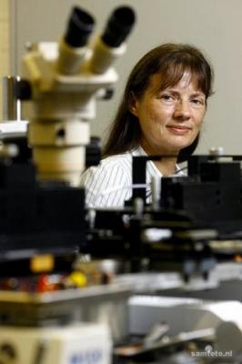
Lis Nanver
Alumnus- Left in 2014
- Now: University of Twente
- Personal webpage
- Google Scholar profile